Everything You Need To Know About Kicad Curved Traces And Advanced Pcb Designs For Electronics Hobbyists - How to make pcb in kicad at ian milligan blog
If you are looking for Macro Photograph of Red PCB with Curved Traces and Gold Vias Stock you've came to the right place. We have 35 Pictures about Macro Photograph of Red PCB with Curved Traces and Gold Vias Stock like Advanced PCB Designs for USB Hub Connectivity, Curved traces in KiCad 5.99 and also The Ultimate Guide to PCB Traces: Everything You Need to Know for. Here it is:
Macro Photograph Of Red PCB With Curved Traces And Gold Vias Stock
 www.dreamstime.com
Macro Photograph of Red PCB with Curved Traces and Gold Vias Stock ...
Electronics For Hobbyists | PCB Tool Expert
 pcbtoolexpert.com
Electronics For Hobbyists | PCB Tool Expert
Melting KiCad - Mitxela.com
 mitxela.com
Melting KiCad - mitxela.com
GitHub - Tiandahuang/kicad-serpentine: KiCAD Extension For Generating
GitHub - tiandahuang/kicad-serpentine: KiCAD extension for generating ...
KiCad 7.0.0 Release - From SpaceMouse Support To Custom Fonts, Here's
 www.reddit.com
KiCad 7.0.0 release - From SpaceMouse Support to Custom Fonts, Here's ...
Vintage Curvy PCB Traces With KiCad 7 - Element14 Community
 community.element14.com
Vintage Curvy PCB Traces with KiCad 7 - element14 Community
Vintage Curvy PCB Traces With KiCad 7 - Element14 Community
 community.element14.com
Vintage Curvy PCB Traces with KiCad 7 - element14 Community
Advanced PCB Design With KiCad: Tips And Tricks | Sierra Circuits
 www.protoexpress.com
Advanced PCB Design with KiCad: Tips and Tricks | Sierra Circuits
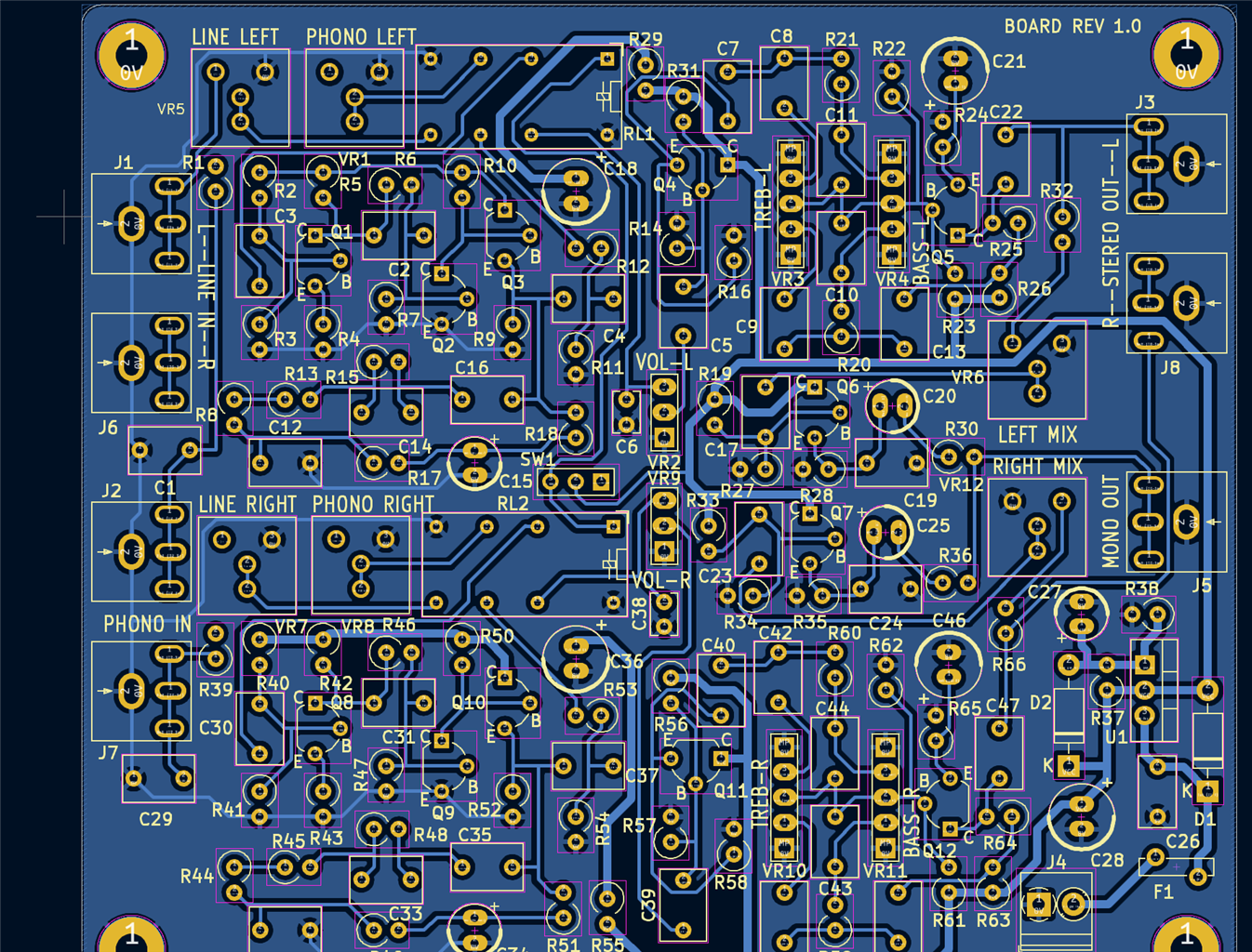
Pads To Kicad At Ken Fatima Blog
 storage.googleapis.com
Pads To Kicad at Ken Fatima blog
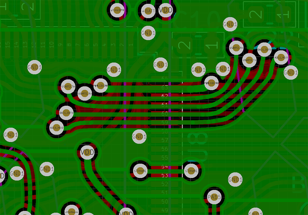
How To Make Pcb In Kicad At Ian Milligan Blog
 storage.googleapis.com
How To Make Pcb In Kicad at Ian Milligan blog
Melting KiCad – Making Curved Traces « Adafruit Industries – Makers
 blog.adafruit.com
Melting KiCad – making curved traces « Adafruit Industries – Makers ...
KiCadの強み/弱み〈強み編〉 - KiCadの達人
 kicad.biz
KiCadの強み/弱み〈強み編〉 - KiCadの達人
The Ultimate Guide To PCB Traces: Everything You Need To Know For
 www.globalwellpcba.com
The Ultimate Guide to PCB Traces: Everything You Need to Know for ...
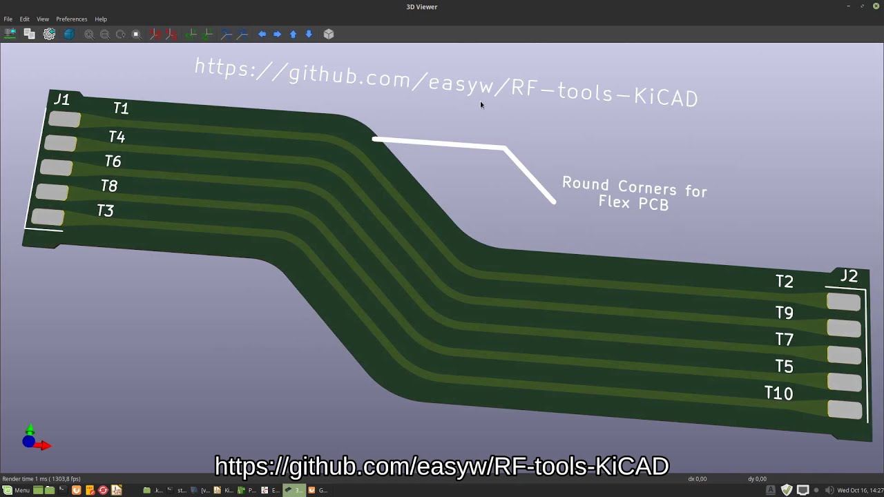
Round Corners Kicad At Callum Fowler Blog
 storage.googleapis.com
Round Corners Kicad at Callum Fowler blog
KiCad PCB Design Step-by-Step Tutorial For Beginners - TechSparks
 www.tech-sparks.com
KiCad PCB Design Step-by-Step Tutorial for Beginners - TechSparks
The Ultimate Guide To PCB Traces: Everything You Need To Know For
 www.globalwellpcba.com
The Ultimate Guide to PCB Traces: Everything You Need to Know for ...
How To Understand Kicad PCB - RayPCB
 www.raypcb.com
How to understand Kicad PCB - RayPCB
Curved Traces In KiCad 5.99
 kbd.news
Curved traces in KiCad 5.99
The Ultimate Guide To PCB Traces: Everything You Need To Know For
 www.globalwellpcba.com
The Ultimate Guide to PCB Traces: Everything You Need to Know for ...
The Ultimate Guide To PCB Traces: Everything You Need To Know For
 www.globalwellpcba.com
The Ultimate Guide to PCB Traces: Everything You Need to Know for ...
The Ultimate Guide To PCB Traces: Everything You Need To Know For
 www.globalwellpcba.com
The Ultimate Guide to PCB Traces: Everything You Need to Know for ...
Advanced PCB Designs For USB Hub Connectivity
 www.enrgtech.co.uk
Advanced PCB Designs for USB Hub Connectivity
Melting KiCad – Making Curved Traces « Adafruit Industries – Makers
 blog.adafruit.com
Melting KiCad – making curved traces « Adafruit Industries – Makers ...
ETA On KiCad 7? : R/KiCad
 www.reddit.com
ETA on KiCad 7? : r/KiCad
Kicad PCB: How To Understand It ? - Jarnistech
 www.jarnistech.com
Kicad PCB: How to Understand It ? - Jarnistech
PCB_ESP32 CSI Curved Traces Resources - EasyEDA
 easyeda.com
PCB_ESP32 CSI Curved traces Resources - EasyEDA
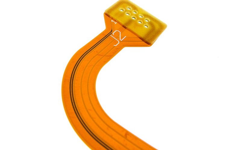
How To Avoid Fracturing Traces In A Flexible PCB Design
 blog.epectec.com
How to Avoid Fracturing Traces in a Flexible PCB Design
How To Design Coplanar Waveguide With Ground In Your PCB: Mastering
 hcjm-pcba.com
How to Design Coplanar Waveguide with Ground in Your PCB: Mastering ...
Kicad 2 Layer PCB Design: Tips And Best Practices – Hillman Curtis
 hillmancurtis.com
Kicad 2 Layer PCB Design: Tips and Best Practices – Hillman Curtis ...
Curved Traces Made With KiCad 5.99 : R/KiCad
 www.reddit.com
Curved Traces made with KiCad 5.99 : r/KiCad
The Ultimate Guide To PCB Traces: Everything You Need To Know For
 www.globalwellpcba.com
The Ultimate Guide to PCB Traces: Everything You Need to Know for ...
The Ultimate Guide To PCB Traces: Everything You Need To Know For
 www.globalwellpcba.com
The Ultimate Guide to PCB Traces: Everything You Need to Know for ...
The Ultimate Guide To PCB Traces: Everything You Need To Know For
 www.globalwellpcba.com
The Ultimate Guide to PCB Traces: Everything You Need to Know for ...
Curved Traces Made With KiCad 5.99 : R/KiCad
 www.reddit.com
Curved Traces made with KiCad 5.99 : r/KiCad
The Ultimate Guide To PCB Traces: Everything You Need To Know For
 www.globalwellpcba.com
The Ultimate Guide to PCB Traces: Everything You Need to Know for ...
How to avoid fracturing traces in a flexible pcb design. The ultimate guide to pcb traces: everything you need to know for .... Advanced pcb design with kicad: tips and tricks